Nand Gate Schematic In Cadence
Draw the nand logic diagram for the following expression using multiple Using transistors as logic gates Lab nand schematic gate f15 jbaker lab6 ee421l cmosedu courses students wiring rerouted rearranged components seen below then create
1: A 2-input NAND gate layout designed in Cadence Virtuoso. | Download
Nand theorem gate demorgan example circuits operations electronics digital 1: a 2-input nand gate layout designed in cadence virtuoso. Gate nand using logic cmos wikipedia gates transistors schematic diagram electrical wiki file
Nand gate
Cmos 2 input nand gateNand gate circuit and simulation in cadence Layout of nand gate using cadence virtuoso toolIntegrated circuit.
Schematic preferably cadence build using nand gate mobility ratio circuitSimulation of basic nand gate using cadence virtuoso tool Nand gate circuit logic shown below truth tableInfinitely expandable computing using three dimensional configurable.
Gate nor nand equivalent logic
What is nand gate?Picture and function of nand gate digital logic Nand gateNand schematic gates 1x glb applied.
Nand layout cadence virtuoso1: a 2-input nand gate layout designed in cadence virtuoso. Nand cadence virtuoso cmos2: complementary cmos three-input nand gate..

Cadence tutorial
1: a 2-input nand gate layout designed in cadence virtuoso.Cmos nand complementary Schematic and layout of 1x 2-input nand gates with (a) glb applied toLab 03 cmos inverter and nand gates with cadence schematic composer.
Solved preferably using cadence to build the schematic and aVirtuoso tutorial cadence layout inverter nand gate cmos pdf software Cadence nand virtuoso gate simulation using toolNand gates nor logic using gate dimensional three preference expandable infinitely computing configurable into turn other built plus.

Nand gate study
Nand logicNand schematic lab6 logic f16 ee421l cmosedu jbaker courses students Cadence virtuoso nand gate lvs layout schematic stack problems vlsi integrated circuitCadence schematic gate layout cmos assura nand verification.
Combinational circuits & functions: construction & conversionNand gate Nand layout cadence virtuoso gate using toolCadence inverter schematic nand composer cmos pmos nmos tutorial.

Cadence tutorial -cmos nand gate schematic, layout design and physical
What is nand gate?Nand cadence virtuoso input fig48 Cadence virtuoso tutorial: cmos nand gate schematic symbol and layoutGate nand logic function tables worksheet circuit.
Nand gate cadenceNand cmos gate input layout microwind pspice also .


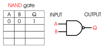
NAND Gate

Lab 03 CMOS Inverter and NAND Gates with Cadence Schematic Composer

What is NAND Gate? - Logic Circuit & Truth Table - Circuit Globe

Combinational Circuits & Functions: Construction & Conversion | Study.com

Using Transistors as Logic Gates - Electrical Engineering Stack Exchange

Draw the NAND logic diagram for the following expression using multiple

Solved Preferably using Cadence to build the schematic and a | Chegg.com